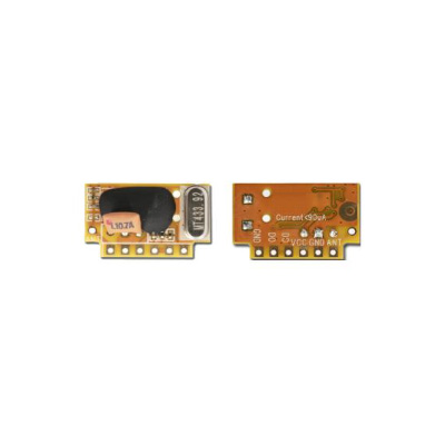
Main features
◆ Super large transmission power
◆ Ultra-high receiving sensitivity
◆ Ultra-small volume
Performance indicators
Output power: 19dBm.
Receiving sensitivity: -115 DBM.
Operating frequency: 315MHz-915MHz.
Operating voltage: 2-3.6V.
Receiving current: 18.5mA.
Emission current: 37mA.
Modulation method: ASK/FSK.
Maximum harmonic: -38 DBC.
Transmission rate: Maximum 100kbps.
Antenna impedance: 50 ohms.
Functional features:
Ultra-low power consumption shutdown mode,
front synchronization signal detection,
digital received signal strength indication (RSSI),
64-byte transceiver data register (FIFO),
timed wake-up function, low power detection,
antenna automatic matching and bidirectional switch control,
temperature sensing and 8-bit analog-to-digital converter,
configurable data packet structure Integrated voltage regulator,
frequency hopping function, power-on reset function,
and built-in crystal adjustment function
Performance parameters:
| Minimum value | Typical value | Maximum value | Unit | Conditions | |
| Operating voltage range | 2 | 3.3 | 3.6 | V | |
| Operating temperature range | -20 | 60 | ℃ | ||
| Receiving current | 18.5 | mA | |||
| Emission current | 37 | mA | @19dBm | ||
| Transmission power range | 1 | 20 | dBm | ||
| Receiving sensitivity | -115 | dBm |
Application:
◇ Remote control ◇ Remote meter reading
◇ Sensor Network ◇ Wireless PC peripheral devices
◇ Tag reader ◇ Tire pressure monitoring
◇ Personal Data Recording ◇ Toy control
◇ Home Automation Telemetry ◇ Health monitoring
◇ Industrial Control ◇ Home Automation Telemetry
Typical circuit:

Module encapsulation:
Foot position definition:
| Pin number | Pin definition | Description |
| 1 | GND | Connect to the power ground |
| 2 | VDD | Connect to the positive terminal of the power supply3.3V |
| 3 | SDN | Turn off the input pin. 0-VDD V digital input. SDN= should be in all modes 0 except the shutdown mode. When SDN=1, the chip will be completely shut down and the contents of the registers will be lost |
| 4 | NIRQ | Interrupt the output pin |
| 5 | NSEL | Serial clock input pins 0 to VDD v, numerical input. This pin provides selection/enable function for the 4-wire serial data bus. This signal is also used to represent burst read and write modes. |
| 6 | SCK | Serial clock input. 0-VDD V digital input. This pin provides a 4-wire serial data clock function |
| 7 | SDI | Serial data input. 0-VDD V digital input. This pin is a 4-wire serial data serial data stream bus. |
| 8 | SDO | 0-VDD V digital output provides serial readback functionality for internal control registers |
| 9 | DATA | Data foot |


